


How we design for EMC
17 December 2025
How we design for EMC
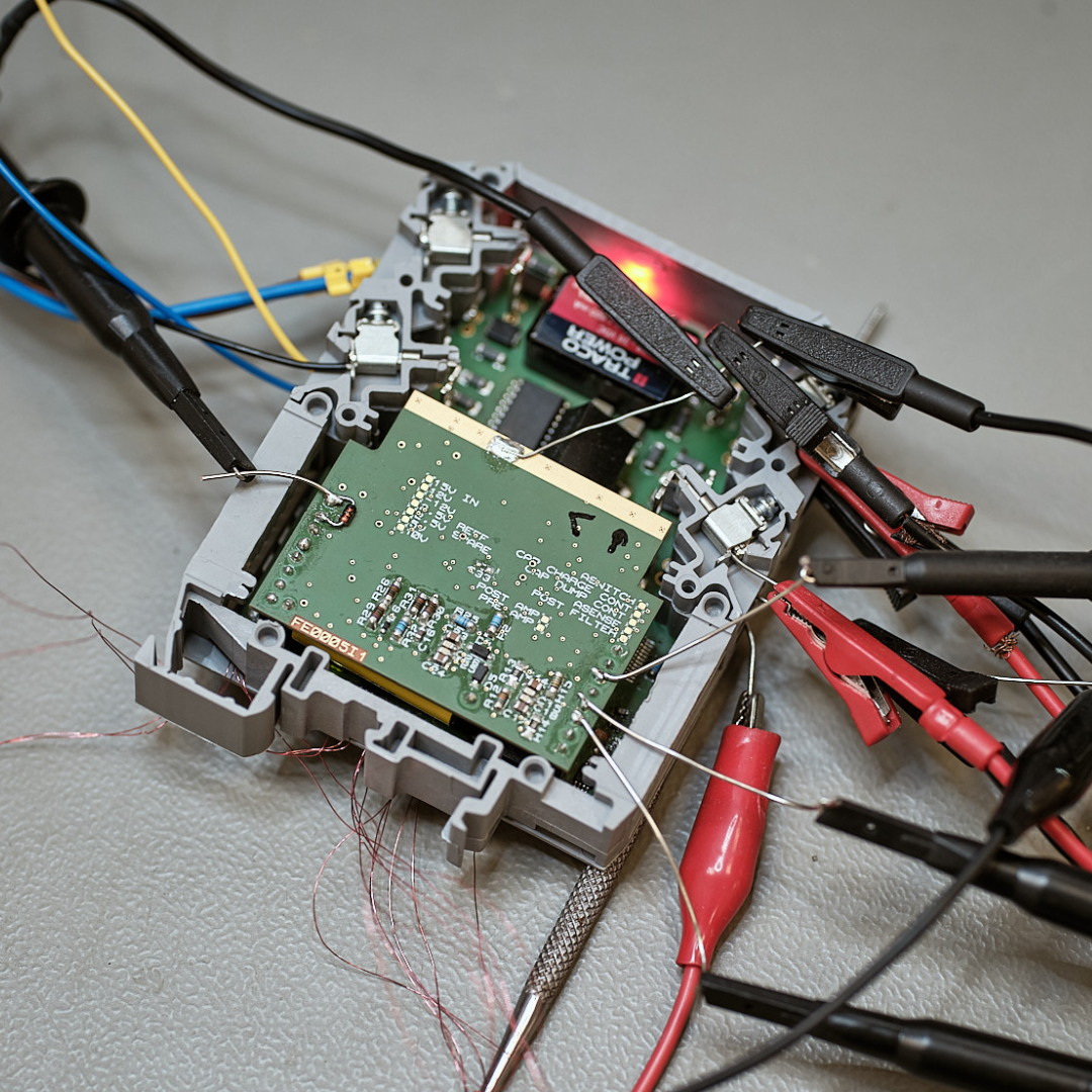
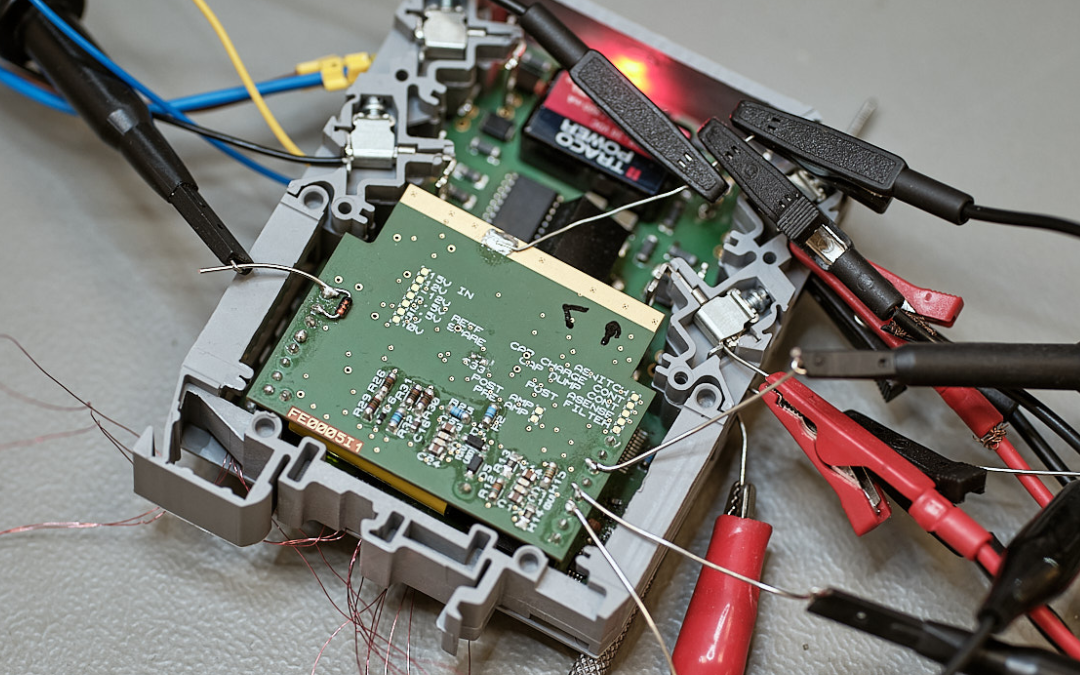
In electronic devices electromagnetic noise sources are everywhere, from switching converters, to clocks and data signals. These can then be radiated by the cabling or traces around it, which act as antennas.
While we are not EMC experts, we do take it very seriously and design for it throughout our entire process, mitigating it in the easiest, safest and most cost effective way possible. The key is to allow for EMC from the start as fixing and rectifying EMC issues after the fact can become hugely complex. The invisible nature of radiation and the expensive nature of booking EMC test lab time, both make debugging your design a job best avoided. So here are some of the ways we make sure EMC issues don’t trip you up.
Pass and fail ranges are based on the classification you’re working to, but the first consideration will generally be the ‘usual suspects’. SMPS – switch mode power supplies – are a very common cause for EMC issues. We will strategically add filtering components such as capacitors, ferites, inductors and resistors. We will also layout our boards carefully to make sure we haven’t made any accidental antennas.
Another thing we may do is design filtering components onto the PCB but leave them unpopulated, so they can be added at the testing stage if required – a much simpler process than trying to solder them on with mods at the lab. Longer cables make excellent antennas for radiating noise – the larger the loop area, the greater the potential to radiate noise. So making sure inductive loop areas are kept small is another simple way to design EMC compatibility in.
Keeping circuits and cables shielded, as in entirely surrounded by grounding in the form of shielded cables, terminals, shielding cans and metal enclosures, keeps our radiation in, and external radiation out. This makes it one of the best solutions for handling radiation and immunity testing, though in the real world it often isn’t possible to take such extreme measures either because of cost or just how the device functions.
Noise won’t radiate if it has somewhere else to go, and a lower impedance path to ground provides that. Designing proper grounding in the form of ground floods on entire layers, shielding noisy traces with ground traces stitched to a ground plane and simply thinking about the path of least impedance for high frequency signals is a simple, cost effective way to manage EMC paths.
Another part of EMC testing is assessing how your device can withstand surges, transients and ESD events. These disturbances can be caused by a wide range of things, such as lightning strikes, inductive load switching, and even you discharging built up static electricity when touching the device. Surges can last a relatively long time and carry high energy while ESD events can reach several thousand volts with extremely fast rise times. To protect our devices against these events we use components such as TVS diodes, clamping diodes and surge resistors along with careful PCB layout to divert and dissipate the energy as heat.
We can monitor how effectively these different techniques are managing noise as we go using simple in-house tools. Then once we are happy we’ve taken it as far as we can, we don’t go straight to testing. Visiting a ‘pre-compliance’ test centre first allows us to get a quick and cost-effective assessment that will identify any red flags.
Once that process is complete we’ll take your design to the full high-cost testing lab for compliance sign-off. We will be there throughout the process, supporting the test team and advising on any fixes that are needed, so you have full technical support and peace of mind throughout.
The end result is a fully EMC compliant PCB as quickly, easily and cost-effectively as possible, ready to get the job done without the risk of non-compliance.

Have a project in mind?
Featured Case Studies

Body Worn Protect Camera
Smart solution to keep frontline workers safe.
Triwave LED Phototherapy head unit
Cool design, inside and out.
Legionella Monitoring System
Keeping Legionella at bay with IOT.